PCB Design Tips
Component Placement
General rule for component placement:
Through-hole (THT) components with polarity must be placed in the same direction, as neatly as possible.
If positioning SMD components in the same direction is not possible, just organize them in the same X or Y direction.
Leave at least 0.5mm in between SMD components, to locate heat sinks.
Thermosensors, such as electrolytic capacitors or crystal oscillators, should be kept far away from high heat elements; and they should be placed on the windward side.

Components with taller figures should be placed behind the shorter components in the direction of the least wind resistance, to prevent air duct from being blocked.
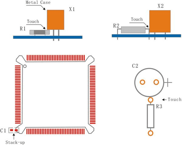
Avoid touching or stacking of components to provide space for component installation.
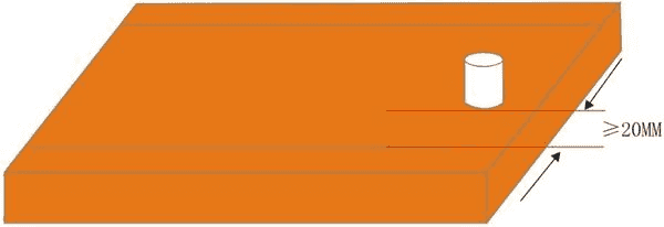
- High heatload components, such as power inductors or power regulators, shoud not be placed to get too close to the technology edge (or panel edge), and the distance to the edge must be above 20mm to avoid uneven temperature of reflow oven guide rail that may affect soldering.
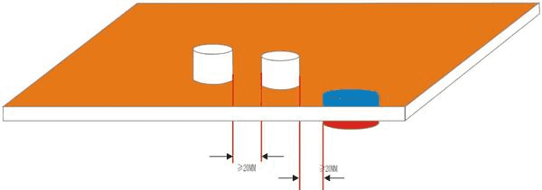
- High heatload components should be at least 20mm apart from each other to avoid large PCB partial heat load.
Through-hole (THT) Component Placement
All polar THT components must be placed on its positive side, unless they are special structural components.
The distance between adjacent components must be at least 0.5mm.

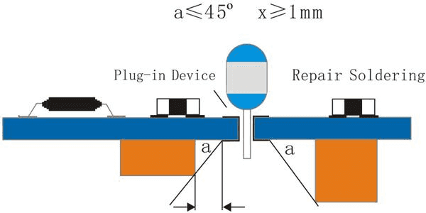
- When SMD components are placed on the opposite side from the THT components, there should be at least 1mm distance between a THT component's leads and the opposite side's SMD component. The angle of elevation ofd the adjacent SMD component's height is at most 45 degrees. The measures are meant to meet the operating space of manual soldering, maintenance and inspection requirements.
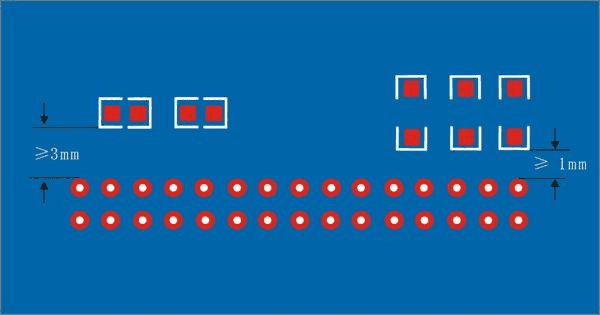
- When SMD components are placed on the same side as the THT components, the pad edge must be at least 3.0mm for parallel placements, and 1.0mm for vertical placements.
Surface-mount Device (SMD) Component Placement
Fine-pitch components (including BGA [insert link!!!], 0.4mm, and 0.5mm QFP) are recommended to be placed on the same side.
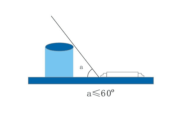
The angle of elevation of SMD components should be less than 60 degrees to ease the soldering joint inspection process.
- BGA components must be at least 3.5mm apart from the next component.

QFN components must be at least 2.0mm apart from the next component.
A surface-mount module must be at least 2.0mm apart from the next component.
SMD with 'wings' or multiple leaded sides, such as SOPs, QFJs, and QFPs should not be positioned on top of each other.
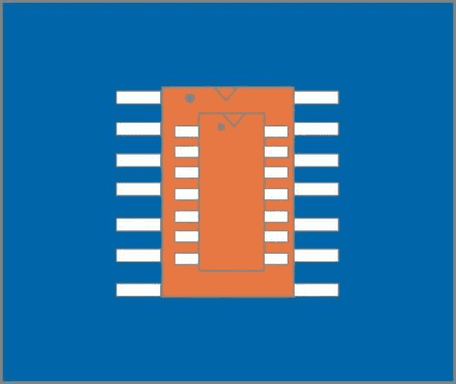
- THT and SMD components can be placed stacked on different layers, as long as the THT soldering does not interfere the SMD pad and the printed solder paste.
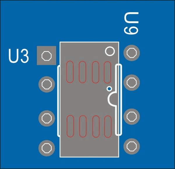
The minimum gap of neighboring SMD components with the same variety is 0.5mm.
The placement of neighboring SMD components of different kinds should have a maximum elevation angle of 60 degrees.
Silkscreen Design
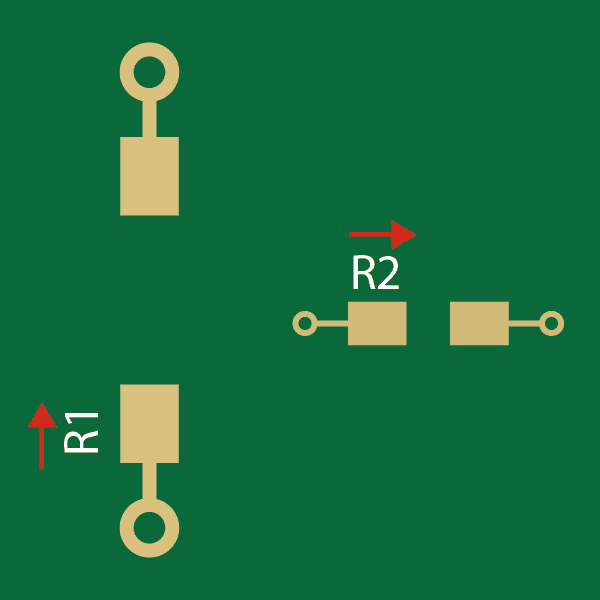
- Annotations written on silkscreen must be written in two direction only: left to right or bottom to top.
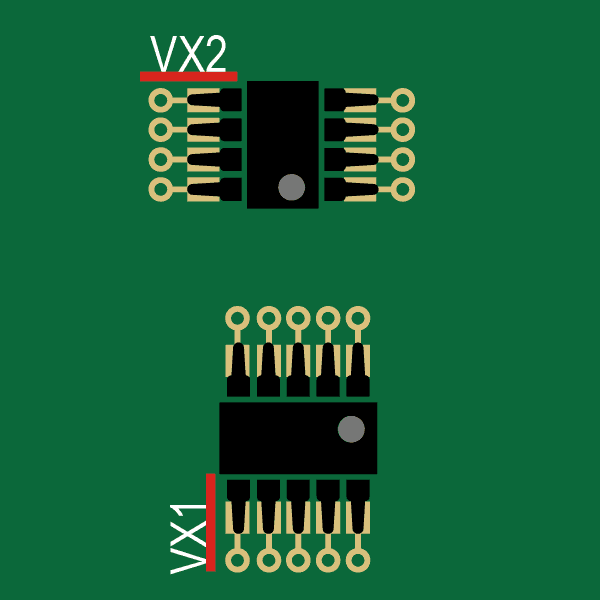
- Place chip annotation on the first leg of a chip component (i.e. the top-left leg or bottom-left leg).
The font width and sizes used should be 4/20mil, 5/25mil, and 6/30mil.
The distance between different annotations or silkscreen elements should be greater than 5mil.
The silkscreen text should be placed close to the corresponding elements to identify them clearly.
When component density is high, annotation could be placed using boxes or arrows to indicate which component the text belongs to.
When the PCB requires high servicability, place annotation under the components. This will deem them invisible once the components are soldered.
Silkscreen should contain information about the mounting hole position and dimensions. This includes screw holes, where the type and length of the screw should also be noted.
The polarity mark (i.e. signal direction) should always be indicated. Additional symbols for polarity indication could be added, since wrong polarity placement is one of the most common reasons for part failure.
Polar components shall placed with the same orientation to reduce human error in manufacturing and quality control.
There should be no silkscreen markings on top of a pad or exposed part. Doing so will reduce the solderability of the pad and will reduce readability alike.
No silkscreen should be present on top of high-speed signal cables to prevent it from negatively affecting the impedance of the cables.
If there are pads enclosed by packaged components such as BGA or QFN chips, the silkscreen should have at least 6mil clearance from the pads.
Connector (such as USB) directions should be clearly indicated on the silkscreen and pin numbers should also be present.
Board name, manufacturing date, version number, and other identifying information should be placed at the corner, with enough clearance from the edge of the board and other components.
Quality verification signs should be added according to related requirements and warning signs for high temperature or pressure should also be added according to your needs.
Company logo, tracking barcodes, QR codes, anti-static markings, etc. are absolutely optional but can be placed at the corner with the other identifying information.
Related Articles
PCB CAD Aperture File Types
Configuring the file types for every PCB design process.
Components
Selecting the appropriate components for your circuits.
PCB Layers
PCBs are made up of layers that fulfill certain tasks. Copper as the conductor, lamination for adhesive, solder mask as the insulation layer, and silkscreen as the guide.
Tolerances & Clearances
The machining process, machining tolerances and clearance requirements for design, manufacturing, and assembly.
