PCB Stencil
PCB stencil plays an important role in PCB layout and SMT. PCB stencils restrict the PCB designs, which also then affects the PCB production rates. Before discussing these issues, we still need to understand its definition and how it works.
A PCB stencil is usually made up of a thin steel sheet that is holed according to the pattern of pads to be engraved in the PCB. A solder paste layer will then be printed onto the stencil, and placed on top of a bare PCB. When pulled out, the solder paste will be on the positions of the pads designed. Next, subsequent patching and flow soldering processes will be continued. In short, a PCB stencil is a mold-like auxiliary tool for printing solder paste.
This being said a PCB stencil is the most crucial part of creating a PCB layout. To understand more about its role, we'll be discussing its own working principles and application scenarios that should be understood first.
Stencil Mesh Design Considerations
In actual design, there are more factors affecting solder paste printing, such as
Types of solder paste
Leaded solder paste is more fluid than lead-free solder paste. Hence, using leaded solder paste will generally shrink the printed pad pattern. Most companies nowadays use lead-free solder paste, in which the mesh-to-pad ratio is 1:1. (i.e., it's assumed there's no solder paste shrinkage).
Solder paste particle size
Solder paste comes in different sizes. When solder paste with larger particle sizes is used for narrow meshes or thin stencils, the amount of solder placed may not be sufficient. Therefore, smaller solder paste particles are usually required for small areas and thin stencils.
Geometry of mesh walls
Irregular geometric shapes, especially sharp angles, will increase the risk of the solder paste coming out patchy. When the printed solder paste is not smooth, the soldering process becomes harder and the components will fall off easily. Therefore, some smaller-sized package pads will be designed as arc pads and rectangular small-sized pads are chamfered or elongated.
Stencil mesh wall smoothness
Most stencils are now being made using the laser cutting process. Thus, the finish of these stencils' walls is generally very smooth, which eases the process of solder paste placement. However, some thicker stencils are still made with a stamping process, which requires an additional polishing process to create a smooth inner wall.
Stencil separation speed
The separation speed of the printing machine will also affect the quality and effect of soldering. Usually, the solder paste used in combination with different placement factories will have some accumulated experience, and will also form a general requirement for the design opening. For example, manufacturer A will request to reduce the opening area, while manufacturer B may request to extend the length, chamfer, or change the shape of the opening for the same product.
Special Cases
As mentioned before, the IPC-7525A stencil design guide can't always be used as a standard design rule set, because in actual production, some special situations should be handled directly based on the handler's experience.
Ground Thermal Pad
The ground thermal pad is usually a large area of copper and needs to be layered with solder paste and flow soldered. In practice, the large area of the solder paste has a strong adsorption force, and the large area is either arched or shrunk into a circle due to surface tension fusion. Therefore, it is usually necessary to shrink inward by 50%-80%, and it is generally designed as a grid mesh.
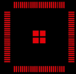
QFP with grounded thermal pad
The QFP with ground thermal pad is a special package. A QFP is made up of numerous surrounding pins around it, the pins will form a lever state with the middle ground thermal pad. The thickness of the solder to be placed might vary for every component.
The speed of heat dissipation is also a crucial point to be taken into account. QFP packages will generally shrink in a grid or a stepped steel mesh should be designed according to the requirements of the specification.

Large size 2-terminal device
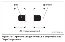
For larger-sized 2-terminal SMD devices including cylindrical MELF components, it is recommended to use the C-shaped (shown in Figure 3-9 of IPC-7525A). By doing so, short circuits -- which are generally caused by solder paste adsorption along the device or solder paste application due to gravity extrusion of the device -- can be avoided

Mesh Production Process
Stencil designs are usually done using EDA software, where it most uses the default packaging rules ratio of 1:1. In practice, chip factories still need to redesign and manufacture the stencil according to the solder paste specifications used, the printing machine, and the manufacturer's experience.
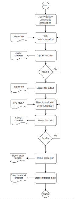
NexPCB has many years of experience in the production and manufacturing of electronic products including the process of stencil design and production workflow as shown in the figure.

