Vias & Holes
In PCB Design, the connection between the board and components, or the connection between individual layers is accomplished by implementing holes. Different types of holes: end-to-end or blind holes, plated or non-plated holes, all serve a specific purpose.
Through Holes
Through holes are commonly used as THT component inserts. NexPCB supports 2 ways of creating through holes:
Mechanical drilling
Laser drilling
Drilled through-holes are differentiated into 2 types: Plated Through Hole (PTH) and Non-Plated Through Hole (NPTH).
Designing Through Holes There are several things to consider when designing through holes:
- The design of through hole needs to meet the requirement that the hole diameter to the panel thickness ratio should be greater than 1/6.
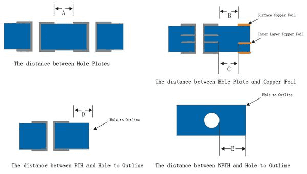
The distance between hole plates is: A ≥ 20mil.
The distance between hole plate and copper foil is: B ≥ 20mil, C ≥ 20mil.
The minimum distance between PTH and hole to outline is the distance that can ensure the distance from the bonding pad to the hole to outline is: D ≥ 20mil.
The recommended minimum distance between NPTH and hole to outline is E ≥ 40mil.
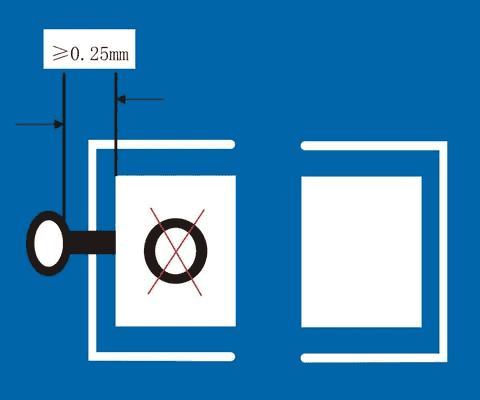
The through holes cannot be designed on a bonding pad, and should be connected by a short printed line.
The minimum distance between a hole wall and a bonding pad is 0.2 mm.
There should be no through holes in the extending outward 1.5 mm area of the contacting part of devices metal shell and PCB.
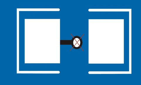
- Through holes cannot be located between two bonding pads meant for one component's placement.
Plated Through Holes (PTH)
Plated Through Holes are drilled through holes that are further processed to be coated with copper. The addition of the copper plating is to:
Provide electrical connections between the PCB layers and the lead of the THT component.
Reduces the connection's resistance (in comparison to copper tracks across PCB)
The process of copper plating is done after the mechanical drilling process. First, the copper is chemically displaced, before electroplating the circuit board to create a thin layer of copper in the walls of the holes.
Non-Plated Through Holes (NPTH)
All holes in PCBs with only one or two layers are Non-Plated Through Holes. The purpose of these holes is to secure THT components into the board, while still maintaining a low production cost. Without a complicated stackup, plating doesn't bring any advantages to resistance.
A location hole is a type of NPTH which serves as an accurate guide to further machining processes, such as drilling the whole stack of boards. These location holes should be placed asymmetrically on the circuit board, to prevent confusion when rotated.
Vias
A via (vertical interconnect access) is a plated hole that allows the current to pass through the board, across different layers and is not used for inserting component leads.
There are a set of rules to be followed when designing vias:
The inner drill diameter of a via is 0.2mm (8mil) and above, and the outer diameter is 0.4mm (16mil) or more.
Vias cannot be placed on pads smaller than the size of the 0402 resistor-capacitance pad
The spacing between the vias should be 0.5mm or wider.
Except for thermal vias, vias with widths ≤0.5mm need to be plugged with oil
BGA fan hole vias should not be on the pads, it is recommended to drill the holes in the middle of the two pads
Via Configuration
Based on how they are organized, vias can be differentiated into 3 types:
Through hole Via
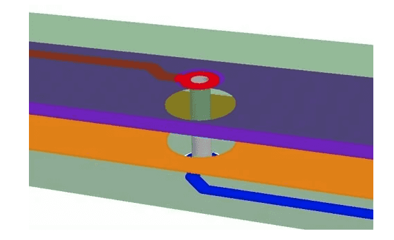
These are used to connect tracks on opposite sides of the PCB (i.e. top to bottom).
Blind Via
In multilayer PCBs, a blind via is commonly used to connect a pad on one end (i.e. top or bottom layer) to an internal layer of the PCB. Hence, it's only visible on one side of the PCB. These connections are usually established to maintain signal integrity and reduce the parasitic capacitance of the PCB.
An ideal blind via must have a minimum of 1:1 ratio between the via depth and diameter.
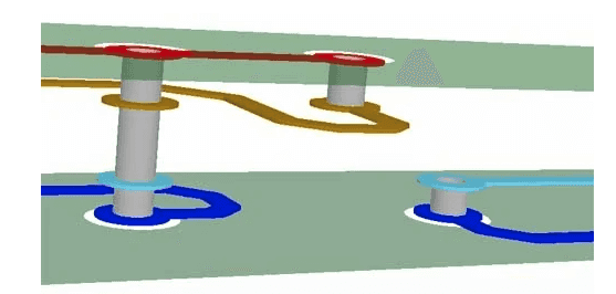
Buried Via
Buried vias are via connections established between the internal layers of a multilayered PCB. Hence, they are not visible on the whole PCB setup as there are no connections to the outer layers.
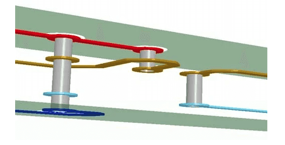
Note: blind via on the right, buried in the middle
Special Vias
Via-in-Pads
Via-in-pads are literally vias created on pads. These vias are excellent for reducing inductance and saving space. They have good thermal dissipation, and don't need any plugging or sealing. However, creating via-in-pads is a rather complicated process, and is more costly than regular via processing.
Microvias
Microvias, are small vias that are usually created with a laser and done before the lamination process. In HDI PCBs, microvias are typically used to allow denser placement of components. They typically have a 1:1 diameter to depth ratio, and hence are formed in a stacked or staggered configuration.
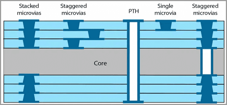
- Stacked Configuration
The stacked configuration occurs when 2 microvias are vertically stacked above each other. These holes should first be drilled separately, before being aligned with an adhesive.
- Staggered Configuration
In staggered configuration, the microvia are not directly stacked on top of each other -- rather staggered. These vias require separate drilling and are glued only after the etching process.
One of the problems caused by these configurations is the generation of EMC radiation. This radiation is caused by the change in the characteristic impedance of the board, due to the short stubs created on the layer where the vias aren't routed. !
Thermal Vias
Another type of vias is the thermal via. Thermal vias are holes that are located under surface-mounted heat-generating components on a PCB. Thermal vias could be of any type: through-hole, in-pad, or microvias. Applicating these thermal vias reduces the thermal resistance of the system.
Tented Vias
Tented vias are generally vias or holes which are covered with a layer of solder paste to reduce the unevenness of the surface. If left unattended, this unevenness could lead to poor SMT processing, and result in changes in the impedance of the circuit board.
Manufacturing Holes and Vias
There are 2 main ways to generate holes and vias:
Mechanical Drilling
The mechanical drilling process is a straightforward process. It uses a drill bit to drill the required depth to form a hole in the board.
Laser Drilling
This method uses either CO2 or YAG UV laser. The process is done by:
CO2 or YAG UV emits laser light beams under the excitation of electrons.
The thermal energy generated by the laser's infrared radiation is absorbed by the resin and glass fiber, which makes up the board.
Copper doesn't absorb this infrared light and hence is not affected.
- The board heats up and melts, forming holes.
Vias Filling
The process of sealing and filling vias is done to solve the problem of the unevenness of the via surfaces. To do this, we could either create a tented via or use a plug hole to fill in the hollow cavities of vias and recessed areas of the surface layer.
The whole process is done to allow soldering to be done on an even surface. When solderingis done on an uneven surface, the change in the circuit impedance could be catastrophic.
There are 3 main processes used by NexPCB to fill vias:
Via Sealing (with solder resist)
Via Plugging (with resin)
Via Filling (by copper plating)
Via Sealing: Solder Resist
Solder resist is the most common via sealing material. The method is done by running the solder resist ink across the top and bottom layers of the PCB.
Using solder resist to seal vias is the simplest and most cost-effective way to complete the task. However, the finish of this process might still be uneven, and could still impact the board's impedance.
Via Plugging: Resin
Vias are plugged with resin, or specific via plugging materials to create an even surface for mounting. The process initially heats the plugged hole to harden the resin, before grinding the excess resin to create a smooth surface. .
The process of via filling is broken down into several steps:
Drilling, creating the initial holes
Deburring and scum removal
Chemical copper plating (immersion)
Copper electroplating
Plugging
Curing, by exposing the board to high temperatures
Using resin plugging to secure vias is a simple and cheap solution, but the heat expansion occurring during the process might cause blisters in the copper layers. To prevent this, the excess resin must first be removed to achieve a flat surface before the etching process.
Resin plugging is most commonly done to vias in HDI circuit boards, where many via-in-pads are used.
Via Filling: Copper Plating
In order to fill the void on the via holes, the copper plating process can further be extended to fill the hole gaps completely with copper. The process will allow the vias to be electrically conductive and have better heat dissipation by adding layers of copper through the electroplating process.
However, the copper plating process is a complex process, which takes up more time and resources than the other methods. Hence, the process is better done only for small holes like microvias.
| Solder resist (Sealing) | Resin (Plugging) | Copper plating (Filling) | |
|---|---|---|---|
| Pros | Cheap Simple process | Low cost Simple process | Electrical conductivity Good heat dissipation Robust |
| Cons | Surface might still be uneven | Might cause copper blisters | Time consuming Complex process Expensive |
| Uses | General usage | Via-in-pad | Microvia |
