PCB Types
Table of Contents
PCBs are the core of all electronic devices. Home appliances, vehicles, mobile phones, tablets, all house PCBs. The space and the working conditions of a PCB inside a toaster, in your car, or inside your smartwatch have very little in common. Therefore, different kinds of materials and manufacturing methods are needed in each scenario.
Standard PCB
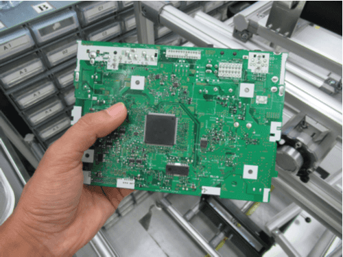
Since their materials and processing are well studied and widely available, they have lower batch production costs and consistently higher manufacturing yields than other types of PCBs.
Here in NexPCB, we provide different materials to construct your standard PCB:
- FR-4
- PTFE
- LDPP
- PP
- Other copper or fiber clad plates, or
- A combination of these materials together, i.e., Hybrid PCBs
| Property | Specifications |
|---|---|
| Layer Count | 2-40 |
| Dimension | Max: 610 * 1100mm Mian: 10 * 20 mm |
| Thickness | 0.2 ~ 8.0mm (±10%) |
Flexible PCBs
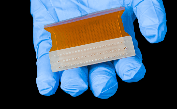
Wearable electronics and consumer devices that are very dense(i.e. Store many components in a limited space), require circuitry that can fit in very limited spaces or in environments where the circuit will be exposed to bending(such as in smartwatches and other wearable devices).
Flexible PCBs are bendable circuit boards, which are made up of light-weight and thin boards. They can be flex-only or come as a hybrid which are called rigid-flex.

Parts of a Flex PCB
The configuration and materials supported for flexible PCB construction are:
- Substrate or base material
This layer is composed of two conducting layers and an insulating layer in between. The commonly used material for substrates is a combination of PI (Polyimide) for the insulating layer and copper for the conducting layers. The layers could be attached together with the help of an adhesive, or bonded together through electroplating, coating, or hot processing methods.
- Cover film
It's composed of release paper, glue, and PI. This layer substitutes the need for solder masks.
- Reinforcement
When needed, flex PCB reinforcements are usually made up of FR4, steel sheet, or PI materials. They are applied after the pasting process and are added through hot pressing or cold pressing methods.
- Other auxiliary materials
Such as glue, electromagnetic protective film, and copper foil.
Rigid-Flex PCBs
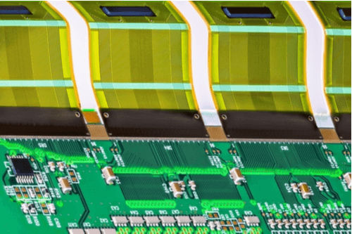
A drawback of having flexible boards is that it's not as robust and strong as standard PCBs. To add strength to these PCBs, the features of the two are merged, creating the rigid-flex PCBs.
Rigid-flex PCBs incorporate both flex and rigid PCBs, either externally or internally depending on the design. This means that they can either be sandwiched together during manufacturing, or can be put together externally using edge connectors. When compared with standard PCBs, rigid-flex PCBs can result with cost savings due to the reduced need for wiring and assembly. However, their fabrication difficulty makes them more expensive. Therefore, an objective cost analysis should be made before deciding on using one in your product.
Designing flex or rigid-flex PCBs in CAD is slightly different from designing standard PCBs. There are a few precautions to be taken into account:
Calculations for layer stacking and impedance control must be adjusted according to the material's processing and thickness of the flexible board.
Annotations and component placement design is done on the cover layer instead of the solder mask as it's done on standard PCBs.
In designing vias, it's important to enlarge the trace, via, annular ring, pad, and spacing as much as possible while still maintaining minimum impedance.
During the addition of a reinforcing layer, a clear description of the layer's position must be indicated.
| Property | Specifications |
|---|---|
| Layer Count | 1-10 |
| Dimension | Max: 200 * 800 mm |
| Thickness | 0.08 ~ 1.0mm (±10%) |
The bending radius and bending cycles of flex and rigid-flex PCBs are as follows,
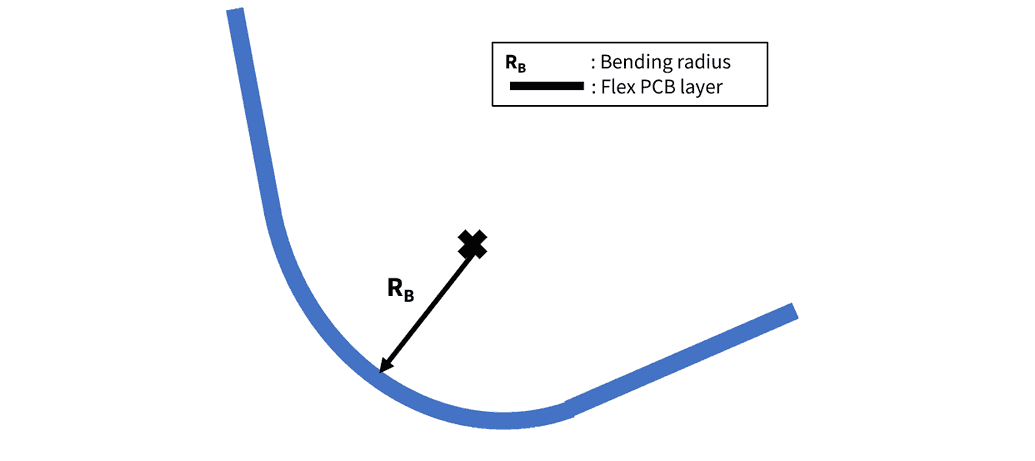
| Bending Radius | Bending Cycles |
|---|---|
| 5 x thickness | 1 |
| 24 x thickness | 100 |
| 250 x thickness | > 10,000 |
HDI PCBs
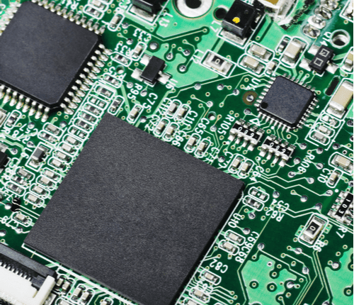
When designing HDI PCBs, there are several options of board materials you can choose from:
FR-4
PTFE
LDPP
PP
Other copper or fiber clad plates, or
A combination of these materials together, i.e., Hybrid PCBs
And RCC (Resin Coated Copper)
With a smaller area, HDI PCBs generally have better signal integrity, since stray inductance and capacitance is reduced. The sizes of HDI PCB's vias are generally smaller than any standard PCB's vias, ranging from around 0.075 mm to a maximum of 0.15 mm.
HDI PCBs are commonly used for PCBs with
Numerous devices
Small dimension
Multiple layers
Many dense high-speed signal traces.
These PCBs are typically implemented for mobile communication purposes and as the motherboard of wearable electronics.
